Special report · The memory bottleneck
The Memory Bottleneck- Room to Think
The scarcest input in the AI buildout is not compute. It is somewhere to keep what a model is thinking about while it waits for you to type. The industry's answer is not one chip but a staircase — fastest and smallest next to the processor, cheaper and slower with every step out — and the next two quarters will show who gets paid on each step.
Thursday, October 1, 2026 · Special report · AI buildout · Five figures
Micron reported its fiscal fourth quarter on Wednesday with an 87 percent gross margin, the vast majority of its calendar 2027 high-bandwidth memory already sold "with significant price increases year over year," and a sentence worth reading twice: it does "not have line of sight to when supply and demand will return to balance" (Micron fiscal fourth-quarter 2026 deck, September 30, slides 13, 17 and 27). It expects conditions "much tighter in calendar 2027 and 2028 than they were in 2026" (slide 16).
Corrections to the first draft of this piece, at full size, after a second fact-check on Thursday. The draft said Micron closed its fiscal year on Wednesday; the year ended September 3 and Wednesday was the report. Five Micron slide citations were off by one and are corrected where they appear. The draft attributed to Astera's chief executive a 2027 volume forecast for Leo X; his forecast was for the Leo CXL controllers, and Leo X was not mentioned on that call. The draft put Marvell's photonic-fabric revenue for next year at "about $150 million"; that was the figure its chief executive framed in May and has since said is rising. The draft credited Nvidia's Dynamo tier names to a blog that does not use them, dated vLLM's cache connector to January when January was the write-up. It gave the wrong baseline for Nvidia's "4x" efficiency claim. Each is corrected in the column.
This morning's Brief called memory the transfer price of the buildout: the one input every builder pays and no builder owns. That is the money question, and it has an answer. This piece is about the question the engineers ask next. Not whether to pay for memory. Where to put the bytes.
A model answering you is holding a conversation in its head. The part it is using this instant has to sit beside the processor, in memory that costs more per gigabyte than anything else in the building. The rest of the conversation — what you said an hour ago, the document you pasted, the ten other people talking to the same machine — has to live somewhere too, and it does not have to live there. Where it lives, how fast it can be brought back, and who sells the shelf: that is the whole design problem of data-center memory in 2026, and it is becoming a market with more than one winner.
The industry's answer is a staircase. Each step out from the processor holds roughly ten times more and moves roughly ten times slower, and costs less per byte in proportion. Nothing on it replaces anything else. The question for an investor is which step the next dollar lands on.
What the model has to remember
For every word a transformer has read in a conversation, it keeps two short lists of numbers in every layer — a key and a value — so that it does not have to re-read the whole conversation to produce the next word. That store is the key-value cache. It grows with the length of the conversation and with the number of conversations the machine is holding at once, and it is the single biggest reason inference now needs more memory than it needs arithmetic.
The arithmetic is simple enough to print. For a model of the shape of Llama 3.1 70B — 80 layers, eight key-value heads, 128 numbers per head, two bytes per number, as published in its configuration file on Hugging Face — the cache is 2 × 80 × 8 × 128 × 2 = 327,680 bytes per token, the desk's arithmetic from the standard formula (Nvidia developer blog, November 17, 2023). At a 131,072-token context, the longest the model accepts, one conversation's cache is 42.9 gigabytes. One hundred such conversations held at once is 4.3 terabytes, before loading a single model weight. That is the memory of fifteen Rubin GPUs, holding nothing but context (the desk's arithmetic; Nvidia lists 288 gigabytes of HBM4 per Rubin GPU).
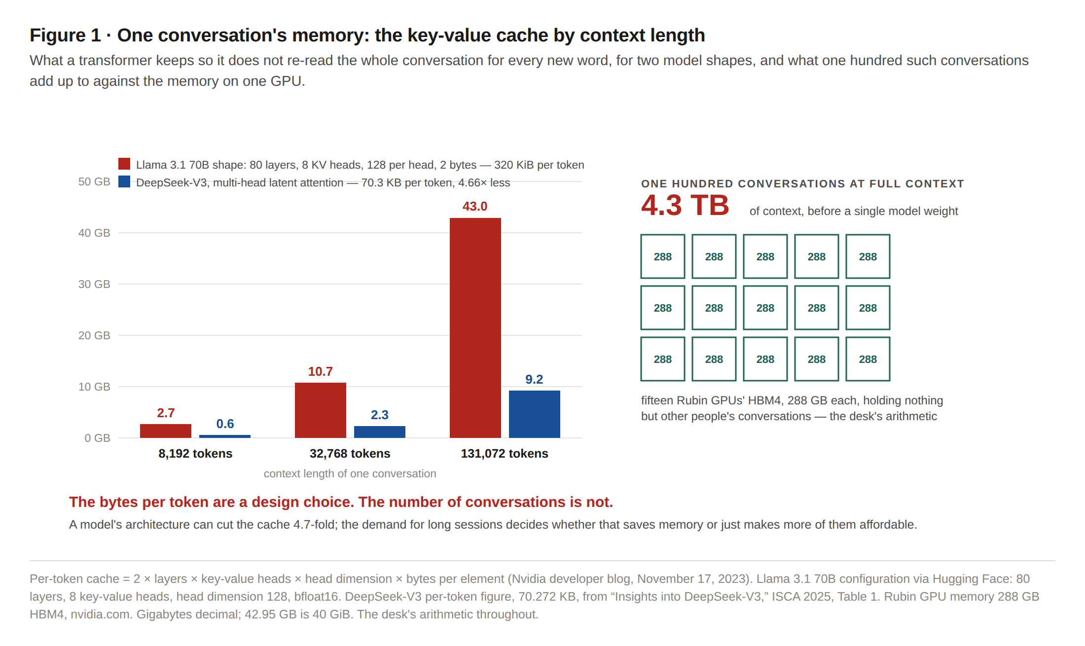
Two things follow, and they pull in opposite directions.
First, the bytes are a design choice. DeepSeek-V3's attention compresses the same store to 70.3 kilobytes per token, by a change in the model's architecture, not in its hardware ("Insights into DeepSeek-V3," ISCA 2025, Table 1, which compares it with Qwen-2.5 72B, a model of the same cache shape as the Llama above, at 327.7 kilobytes). Against the Llama shape, that is 4.66 times smaller, the desk's arithmetic in the same two-byte precision. Quantizing the cache to fewer bits cuts it further. However, Hugging Face's own documentation warns that doing so "can harm latency if the context length is short and there is enough GPU memory available for generation without enabling cache quantization." Any memory-demand forecast that assumes bytes per token are fixed is assuming the one thing the model builders are most actively changing.
The second is that the bytes are worth keeping. Moonshot AI, which serves the Kimi chatbot, published the architecture of its serving system last year under a title that is the thesis of this piece in six words: "Trading More Storage for Less Computation." It stores the cache across the cluster's "CPU, DRAM, SSD and NIC resources" rather than recomputing it. It reports that doing so "increases the effective request capacity by 59%~498%" depending on the workload (Qin et al., USENIX FAST 2025, best paper). A conversation's context has become inventory. Inventory needs a warehouse, and warehouses are a business.
Micron now lists that business by name. "AI context memory storage used for KV cache offload and HDD displacement opportunities are expanding the addressable market for SSDs," the company says, and its data-center SSD revenue in the quarter just reported was "nearly $10 billion, more than 10 times the year-ago quarter" (deck, slide 13). The cheapest shelf in the warehouse is flash, and it is already a nearly ten-billion-dollar quarter, though not all of that is context.
The staircase
Begin at the top. A Rubin GPU carries 288 gigabytes of HBM4. Nvidia's specification table for the Vera Rubin NVL72 rack, updated Wednesday, puts the bandwidth at 19.2 terabytes a second per GPU; the company's own developer blog from July says "up to 22 TB/s." Both are Nvidia's figures, and the desk prints both (nvidia.com Vera Rubin NVL72 page; Nvidia developer blog, July 21). AMD's MI455X lists 432 gigabytes at 23.3 terabytes a second (amd.com). One Micron HBM4 stack moves "greater than 2.8 TB/s" over a 2,048-pin interface, twice the width of HBM3E (micron.com HBM4 page; Micron release, March 16).
That is the fire main. Everything below it is a hose.
Beside the CPU, Nvidia's Vera carries "up to 1.5 TB" of LPDDR5X at up to 1.2 terabytes a second (nvidia.com Vera CPU page); Micron, which supplies the modules, describes SOCAMM2 as "enabling up to 2TB of memory and 1.2 TB/s of bandwidth per CPU" (Micron release, March 16) — two vendors, two capacities, printed as found. Behind a PCIe 6 slot, a CXL memory expander offers terabytes at about 120 gigabytes a second each way. Behind an Ethernet port, a flash tier offers petabytes at tens of gigabytes a second per GPU. Each step out is roughly an order of magnitude more room and an order of magnitude less speed, the desk's reading of the vendors' own figures.
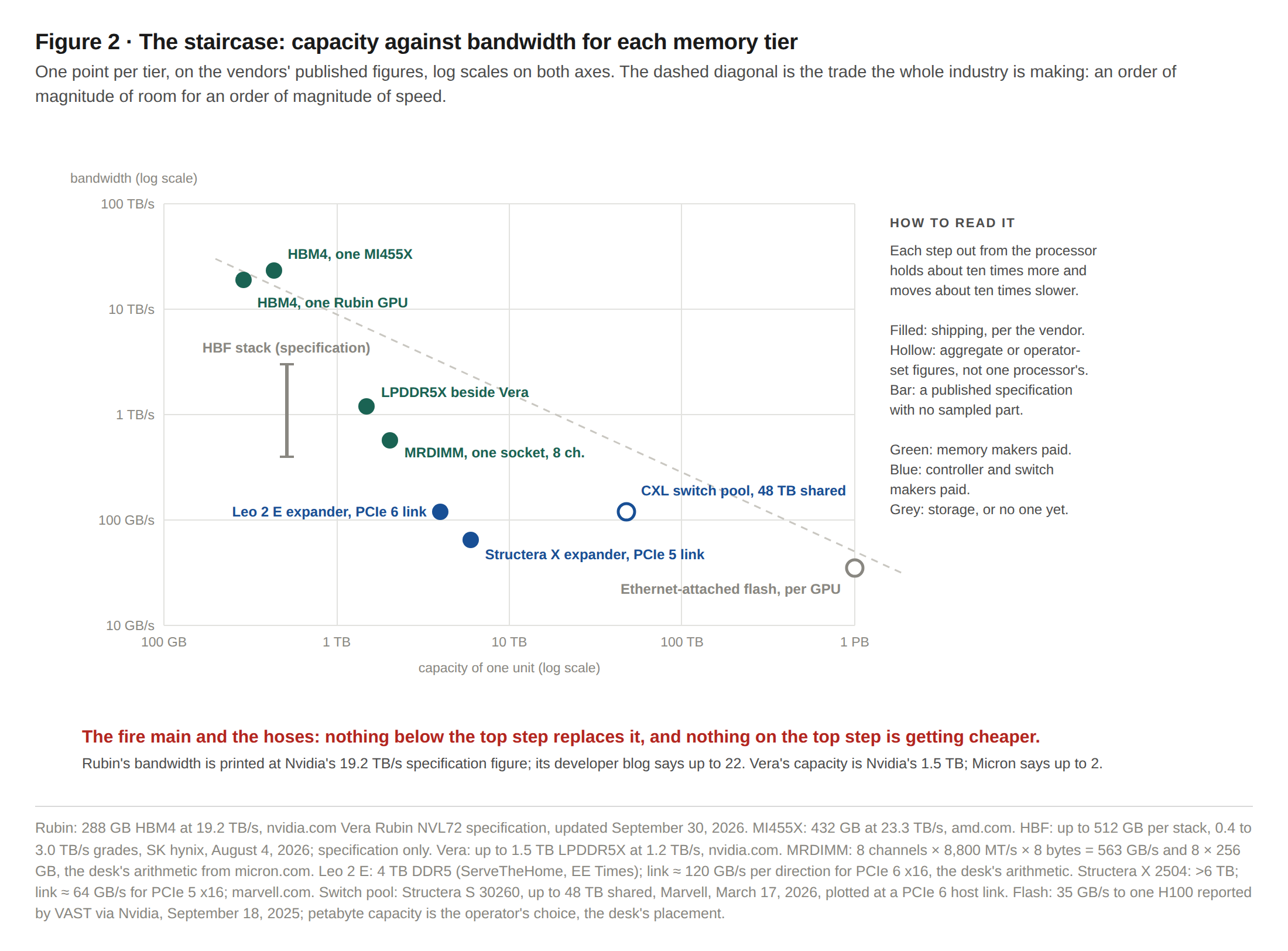
The staircase exists because it's the oldest fact in computer architecture, and it is getting worse. Peak server compute "has been scaling at 3.0x/2yrs, outpacing the growth of DRAM and interconnect bandwidth, which have only scaled at 1.6 and 1.4 times every 2 years" — 60,000-fold, 100-fold and 30-fold over twenty years (Gholami et al., "AI and Memory Wall," IEEE Micro 2024). Processors have outrun memory, and memory has outrun the wires. Every product in this piece is an attempt to put the right bytes on the right step.
The first step out: more memory beside the processor
The cheapest fix is the one that changes the least. Make the local tier bigger and faster, and some of the problem goes away before anyone has to buy a new kind of hardware.
That is what SOCAMM2 is — a small, low-power module that puts phone-class memory beside a server CPU. Micron put the 192-gigabyte part into "high-volume production" in March, in a range "spanning 48GB to 256GB capacities," designed "for NVIDIA Vera Rubin NVL72 systems and standalone NVIDIA Vera CPU platforms" (Micron release, March 16). It is what multiplexed-rank DIMMs are, too: Micron's MRDIMM runs "up to 8.8K MT/s," and the company measures "up to a 39% improvement in bandwidth" against a DDR5-6400 module of the same size, in its own published test (micron.com MRDIMM page). The desk's arithmetic: eight channels at 8,800 megatransfers and eight bytes each is 563 gigabytes a second per socket, against 410 for DDR5-6400. A second generation "is currently under definition by JEDEC" (same page); trade coverage puts its target at 12,800 megatransfers (TweakTown, May 5, secondary).
It is also, in a sense, what Rubin CPX is: a GPU with 128 gigabytes of GDDR7 instead of HBM, built for the part of inference that reads a long prompt rather than the part that writes the answer, due at the "end of 2026" (Nvidia release, September 9, 2025) — different memory for a different phase of the same job.
This step is what memory makers get paid for first, and it is why Micron's margin is where it is. TrendForce expects conventional DRAM contract prices to rise another "10–15% QoQ in 4Q26" (September 30). Nothing on the staircase below this step removes a gigabyte of demand. It only decides where the next gigabyte goes.
The second step: memory that is not in the server
Compute Express Link is the industry's standard for letting a processor use memory that is not on its own motherboard — on a card, or in another box — over the PCIe wiring servers already have. It is three protocols on one wire: one for finding and configuring devices, one that lets a device cache the host's memory, and one that lets the host read and write memory on the device. A plain memory expander uses the first and the third and is called a Type 3 device (Linux kernel documentation, CXL device types). A reader who remembers only one thing about CXL should remember that it is a standard, not a product, and that the standard runs years ahead of the hardware: CXL 4.0, announced November 18, 2025, "doubles the bandwidth to 128GTs with zero added latency," and the desk could find no silicon that implements it — only licensable design blocks (CXL Consortium release; StorageReview, August 8, on Synopsys's design blocks).
The hosts that can use it today, by their own specifications: AMD's Turin, with "up to 64 lanes" of CXL 2.0 (AMD white paper, March 2025); Intel's Xeon 6, with "up to 64 lanes of CXL 2.0" (product brief, May 13); and Nvidia's Vera, which lists "Gen6/CXL 3.1" and which Nvidia says "begins shipping at scale" (developer blog, January 5, updated August 21; Nvidia blog, August 27). AMD's Venice, also CXL 3.1, is "ramping production," with partner systems reported due in the fourth quarter (AMD, May 21; StorageReview, July 23, secondary). The link itself is the constraint to keep in mind: a PCIe 5 x16 slot carries about 63 gigabytes a second in each direction and a PCIe 6 slot about 120, the desk's arithmetic from PCI-SIG's rates and the 256-byte packet format (118 to 121 depending on what one counts as payload). An HBM4 stack moves 2.8 terabytes a second. CXL is for room, not speed.
Does the room cost performance? The published tests say: for some workloads, with care, not much. Intel's February 25 technical paper ran a MongoDB benchmark on a two-socket server with a terabyte of DRAM per socket, then again with half of it replaced by CXL memory and the hardware managing which data lived where, and found throughput "just 1–3% lower" on a 90-percent-read workload (Intel technical paper 886601). An OSDI 2024 paper from Columbia, Microsoft Azure, Intel and others, on a full-system prototype, found "no more than 5% degradation for more than 82% of workloads" — and outliers that degraded by up to 34 percent until a smarter allocator brought them "below 6%" (Zhong et al., USENIX OSDI 2024). A Micron-Intel white paper that spread memory traffic across eight Micron CXL modules and the local channels found read-only bandwidth up 24 percent and mixed traffic up "up to 39%" (Intel white paper 842211; arXiv 2412.12491). These are the vendors' and the labs' own tests, on their own workloads. They establish that the step exists. They do not establish that any particular application will take it without noticing.
One cloud has taken it in public. Astera Labs' Leo controllers went into Microsoft Azure's M-series virtual machines in private preview on November 18, 2025 — "the industry's first announced deployment of CXL-attached memory," in Astera's words, at "up to 2TB" per controller (Astera release). The desk found no announcement of a public preview or general availability.
The hardware on this step is now a second generation. Astera's Leo 2 E-Series, announced September 15, attaches "CXL 3.2 memory expansion via PCIe 6 x16"; the P-Series handles "pooling and sharing across hosts" over two x8 ports with "dynamic capacity management"; both carry "four DDR4 or DDR5 memory controllers," and "the family is sampling today with hyperscaler customers" (Astera release, September 15). Trade reports put the capacity at 4 terabytes of DDR5 or 768 gigabytes of DDR4 per controller (ServeTheHome, September 15; EE Times, September 29; both secondary). Marvell's Structera X 2504 carries more than 6 terabytes of DDR5 and "up to 200 GB/s" of memory bandwidth behind a PCIe 5 x16 host link that moves about 63 — the number on the box is not the number through the door (marvell.com; the desk's arithmetic) — and Marvell's chief executive said on August 27 that the technology is "now getting deployed at multiple hyperscalers with varying architectures by the way, in extremely high volumes" (Q2 fiscal 2027 call, Motley Fool transcript, secondary). Samsung sells a CXL 2.0 module at 128 and 256 gigabytes and lists a CXL 3.2 part on its product page; its next generation is due "by the end of this year" by one Korean report, on a CXL 3.2 module, and in the first quarter of 2027 by another, on a CXL 3.1 module (TrendForce, July 21; The Elec, July 7; both secondary, and possibly about different parts).
Then there is the part of the pitch the desk finds most interesting, because it is the only new supply in this piece that no fab has to build. Astera's new controllers include "purpose-built memory test engines and automated repair engines" to "identify reliable DIMMs for reuse" (release, September 15) — old DDR4, pulled from retired servers, tested and put behind a controller a new server can read. Thad Omura, Astera's senior vice president for compute connectivity, told EE Times: "That stranded DRAM is the industry's next scale-up resource" (September 29).
The spot market says why. On September 30, TrendForce's spot sheet had a 16-gigabit DDR5 chip at $57.90 and a 16-gigabit DDR4 chip at $83.69 — $28.95 and $41.84 a gigabyte, the desk's arithmetic. Old memory costs 45 percent more per gigabyte than new memory. The spot sheet doesn't say why; the desk reads it as the fabs' wafers having shifted to DDR5 and HBM, which is what the wafer-share figures below describe. In that market, a controller that makes a tested used DIMM usable again is not a connectivity product. It is a memory supplier that does not need a cleanroom.
Here is what the step cannot do yet, from the one source with no product to sell. The Linux kernel's own CXL maturity map, in the current documentation, marks as "known gap" the fabrics chapter of the specification, hardware-coherent and software-managed shared memory, dynamic capacity devices, and every accelerator (Type 2) item; hotplug is "stabilizing" (docs.kernel.org, CXL maturity map, 7.3-rc5 documentation; a patch dated April 17 would raise other items — soft-reserved conflicts, switch protocol errors, scrub, repair and sparing — and had not landed in the published docs at this writing). The consortium's own webinar note says the same in its own voice: "The exact performance depends on the design, configuration, and traffic," and pooled memory requires that "the software must be NUMA optimized, which takes time and effort" (CXL Consortium, January 15, 2026).
So the honest division of this step is: expansion — more memory for one server — is shipping, in volume, to named buyers. Pooling and sharing — the part of the pitch where a data center buys memory separately from servers and hands it around — is a specification with early hardware and a kernel that does not yet fully support it. The economic idea everyone quotes, buy compute when you need compute and memory when you need memory, belongs to the second half.
The third step: a memory tier that belongs to the accelerators
The second step attaches memory to a CPU. The third attaches it to the GPUs' own fabric, so that a cache being paged back for a conversation never has to cross the CPU's memory system at all.
Astera's Leo X-Series is that product, and it is not a CXL expander. Astera calls it "fabric-attached," pairs it with its Scorpio switches "using PCIe and platform-specific protocols for scaling up GPUs," and describes its purpose as "a dedicated memory tier for offloading KV cache and agent context" (release, September 15). The headline numbers are "up to 62% faster time to first token (TTFT) and up to 22% more tokens per second." The footnote matters: "As measured by Astera Labs internal testing" on a server "with 8 DDR5 memory channels populated, using a data center Gen 5 AI accelerator on the Qwen2.5-32B AI Model" — four H200 GPUs, per EE Times — against conventional offload to the CPU's own DRAM (release; EE Times, September 29).
A correction to the desk's draft, in full. The draft carried millisecond figures for that test — 246 against 127 for a warm turn, 413 against 158 under artificial memory contention, 32 stressor threads, ten 32,000-token sessions, a patched LMCache — attributed to Astera's technical blog. The desk could not retrieve that page; it loops between addresses at this writing, and no second source carries the figures. This piece prints only the release. If the draft's numbers are right, the 62 percent is the contended case, and the uncontended gain is 48 percent, the desk's arithmetic — which is the honest version of the claim, and a smaller one.
The test demonstrates one real thing: that a cache kept off the CPU's memory bus does not have to wait in line behind the CPU's other work. It does not demonstrate HBM-class performance, and it does not demonstrate production. Leo X is sampling. The nearest thing to a volume date is for its CXL siblings: Astera's chief executive expects "to ship both standard and custom Leo CXL memory controllers in volume" to "two U.S. hyperscalers" in 2027, on a call six weeks before Leo X existed in public (Q2 2026 call, August 4, Motley Fool transcript, secondary).
The switch is further along. Scorpio X, expanded to 320 lanes on May 5, is what Astera calls "the industry's largest open, memory-semantic fabric switch," with "hardware-accelerated Hypercast and In-Network Compute engines" that "boost collective operations by up to 2x" — a figure the footnote defines as "at least 50% reduction in AllReduce collective operation latency compared to traditional Ring AllReduce," not a doubling of anything an application would see (Astera release, May 5). It is "shipping today," and the company expects Scorpio to become its largest product family in the quarter that ended Wednesday, "one quarter ahead of our prior expectations" (Q2 release, August 4). That is the near-term money on this step: the switching, not yet the memory.
Marvell's version runs through CXL. Its Structera S 30260, announced March 17, is "a new 260-lane CXL switch device" with "CXL 3.0 support and aggregate bandwidth up to 4TB/s," connecting "16 or 32 CPUs or GPUs" to "up to 48TB of shared memory" at "less than 460ns for round trip memory access through the switch," and was "expected to begin sampling to customers in calendar Q3 2026" (Marvell release, March 17; the capacity and latency figures are from Marvell's blog of the same day). The quarter ended Wednesday. The desk found no confirmation that sampling began — not in the August 4 memory release, the August 27 call, or the September newsroom — and the earlier S 20256, a CXL 2.0 switch, "is currently in production." A reader should hold the 4 terabytes a second the way the Marvell expansion bandwidth is held above: that is the switch's total, not any one processor's share.
The far end of this step is optical. Marvell's Photonic Fabric, announced August 4 in the same release as its memory line, "creates a new shared-memory tier across multiple XPUs and racks up to 50 meters, enabling up to 32TB of warm KV cache offload," with "up to 2-3x higher token throughput" (Marvell release, August 4). It is the product of Celestial AI, a purchase announced on December 2 at "approximately $3.25 billion" up front with up to $2.25 billion more on revenue targets, and closed February 2 (Marvell releases). Marvell's chief executive framed the fabric's revenue for next year at "about $150 million" in May and said in August that the figure is "accelerating even further" (May 27 and August 27 calls, Motley Fool transcripts, secondary). Fifty meters is the length of a rack row. Thirty-two terabytes is the context of about 745 long conversations of the Llama shape, the desk's arithmetic. Neither number is a deployment.
The fourth step: flash learns to remember
The cheapest byte in the building is on an SSD, and in January Nvidia gave it a job title.
At CES on January 5, Nvidia announced an "Inference Context Memory Storage Platform" built on its BlueField-4 processor; at GTC on March 16 it renamed the layer CMX and published a reference design, STX, around it (Nvidia releases, January 5 and March 16). The idea is an Ethernet-attached flash tier that Nvidia's engineers label "G3.5" — between local SSDs and shared storage, in their numbering — "optimized specifically for KV cache," with the inference frameworks doing the clever part: "KV managers in these frameworks prestage KV blocks, bringing them from CMX into G2 or G1 memory ahead of the decode phase" (Nvidia developer blog, March 16). Prestage is the operative word. The flash is slow. The trick is to ask for the conversation back before the model needs it.
Nvidia claims "up to 5x" tokens per second against conventional storage and "4x higher energy efficiency compared with traditional CPU architectures for high-performance storage," names a dozen storage partners from Dell and NetApp to VAST and WEKA, three manufacturers, and eight AI labs and cloud providers "planning to adopt" it, including CoreWeave and Mistral, with availability in the second half of 2026 (GTC release, March 16). The partners' own numbers are the vendors': DDN claims "up to 27x faster KV cache loading," WEKA "4-10x more tokens per second" (Blocks & Files, March 30, secondary). In Nvidia's Dynamo framework, the tiers already have names — G1 for GPU memory, G2 for pinned CPU memory, G3 for local SSD, G4 for remote storage (Dynamo KV block manager design document) — and the published partner results show what the hose delivers: VAST reached "35 GB/s throughput to a single NVIDIA H100 GPU," WEKA "read throughput up to 270 GB/s" across eight (Nvidia developer blog, September 18, 2025).
Flash's next move is to climb the staircase rather than wait at the bottom. High Bandwidth Flash stacks NAND the way HBM stacks DRAM and puts it beside the processor. On August 3, Sandisk and SK hynix published the first HBF specification through the Open Compute Project, covering "basic performance expectations, the xPU-HBF host interface, reliability and packaging guidance for an HBF die stack, and a software user guide," with Google and Tenstorrent joining as consortium members (Sandisk release, August 3). SK hynix describes stacks of "up to 512GB" with bandwidth grades of "approximately 0.4TB/s to 3.0TB/s" (SK hynix newsroom, August 4). The pitch is "8-16x the capacity" of HBM at HBM-adjacent bandwidth for data that is read far more than it is written — which is exactly what a conversation's context is (Sandisk-SK hynix memorandum, August 6, 2025).
A second correction at full size. The draft carried the memorandum's timeline: first HBF samples in the second half of 2026 and samples of the first inference devices in early 2027. At its August 13 investor day, Sandisk showed a taped-out die and listed its first HBF inference product samples as "coming soon, 2027" (StorageReview, August 18, secondary). The schedule slipped. A specification published in August and a sample due next year is an ecosystem milestone and nothing more; it is the only thing on the staircase that could change the economics of the top step, and it is the furthest from doing so.
The cost of distance
The staircase is only useful if the reader keeps one quantity in mind, so the desk did the arithmetic once. Take one conversation of the Llama shape at full context, 42.9 gigabytes, and move it across each link at that link's published ceiling.
Through HBM4 on a Rubin GPU, at 19.2 terabytes a second: two milliseconds. Through Vera's LPDDR5X, at 1.2 terabytes a second: 36 milliseconds. Through a PCIe 6 x16 slot, at about 120 gigabytes a second: just over a third of a second. Through a PCIe 5 x16 slot: two-thirds of a second. From Ethernet-attached flash, at the 35 gigabytes a second VAST reached to one H100: one and a quarter seconds. Real transfers are slower than ceilings. The ratios are the point.
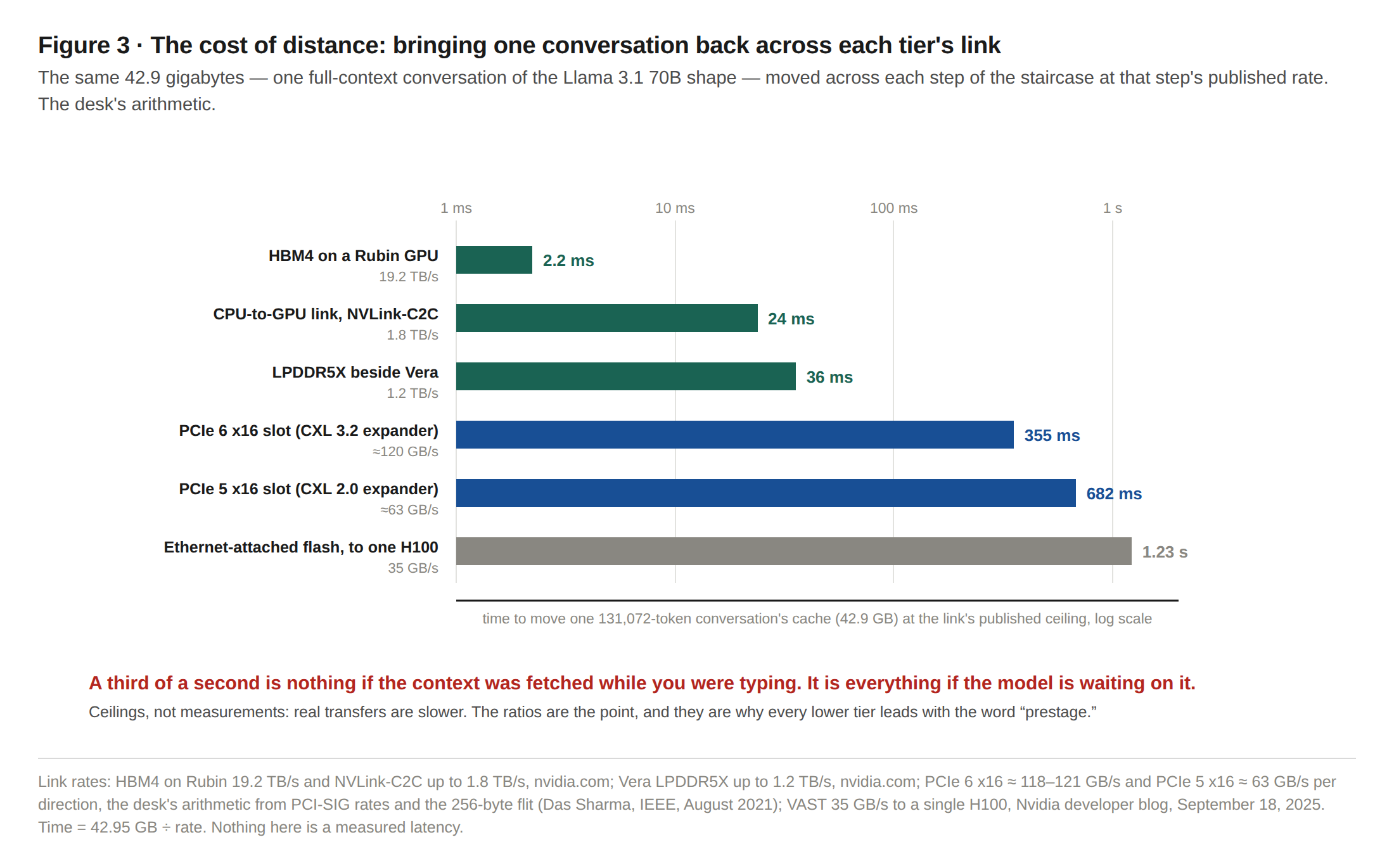
A third of a second is nothing if the context was fetched while you were typing your question. It is the whole user experience if the model is waiting on it. That is why every product on the lower steps leads with the same word — prestage, prefetch, warm — and why the software that decides what to fetch, and when, is worth more than the link it fetches over. It is also why a switch's aggregate bandwidth and a pool's total capacity are the least useful numbers in any of these announcements. The question is never how big the warehouse is. It is how long the walk is.
The software that moves the wall
Code can move every step of the staircase in both directions.
vLLM, the most widely used open inference engine, introduced a connector in version 0.11.0 last fall that keeps the cache in CPU memory, and in January reported that "loading KV values from the CPU reduces TTFT by X2-X22" with throughput "up to X9," on an 8-billion-parameter model on an H100 (vLLM blog, January 8). LMCache, the layer Astera patched for its test, claims "3-10x delay savings" in multi-turn and retrieval workloads and "up to 15x" throughput in its technical report (LMCache README, via a mirror; arXiv 2510.09665). Those are software gains on hardware that already existed. They are the reason a hyperscaler's first move is a configuration change, not a purchase order.
And the architecture moves faster than either. DeepSeek's compression of the cache — 4.66-fold against the Llama shape, the desk's arithmetic — is one choice; sliding-window attention, which "only keeps the last `sliding_window` tokens," is another; sharing a common prefix across conversations is a third (Hugging Face cache documentation). Each one shrinks the warehouse the staircase is built to serve. Each one also makes a long conversation cheaper, which makes more people have one. The net of those two is not predetermined, and anyone who tells you the direction is guessing.
What the desk will say is this: the bytes per token are falling and the tokens per day are rising, and so far the second has outrun the first. Micron's nearly ten-billion-dollar SSD quarter is the evidence. If the software ever wins, it will show up there first.
What is real, and what is a bet
Sorted by what the sources establish, not by what the announcements say.
Shipping in volume, with named buyers or reported revenue: HBM4 (Micron, volume shipment from the first calendar quarter; SK hynix, "mass shipments" from the second; Samsung, from February); SOCAMM2 and MRDIMMs; CXL memory expansion behind Marvell's controllers ("extremely high volumes," per its chief executive) and Astera's first-generation Leo (Azure, private preview); Scorpio X at 320 lanes; Marvell's CXL 2.0 switch.
Sampling or previewing, with a date attached: Leo 2 and Leo X (sampling since September 15; volume 2027); CMX and STX (availability second half 2026); AMD's CXL 3.1 hosts (ramping; platforms reported due this quarter); Samsung's next CXL module (year-end or first quarter, depending on the report).
Announced, with no confirmed sample: Marvell's 260-lane CXL 3.0 switch (target quarter passed Wednesday); Photonic Fabric (first revenue next year, by Marvell's own account); HBF (samples 2027); CXL 4.0 (specification only; no silicon found).
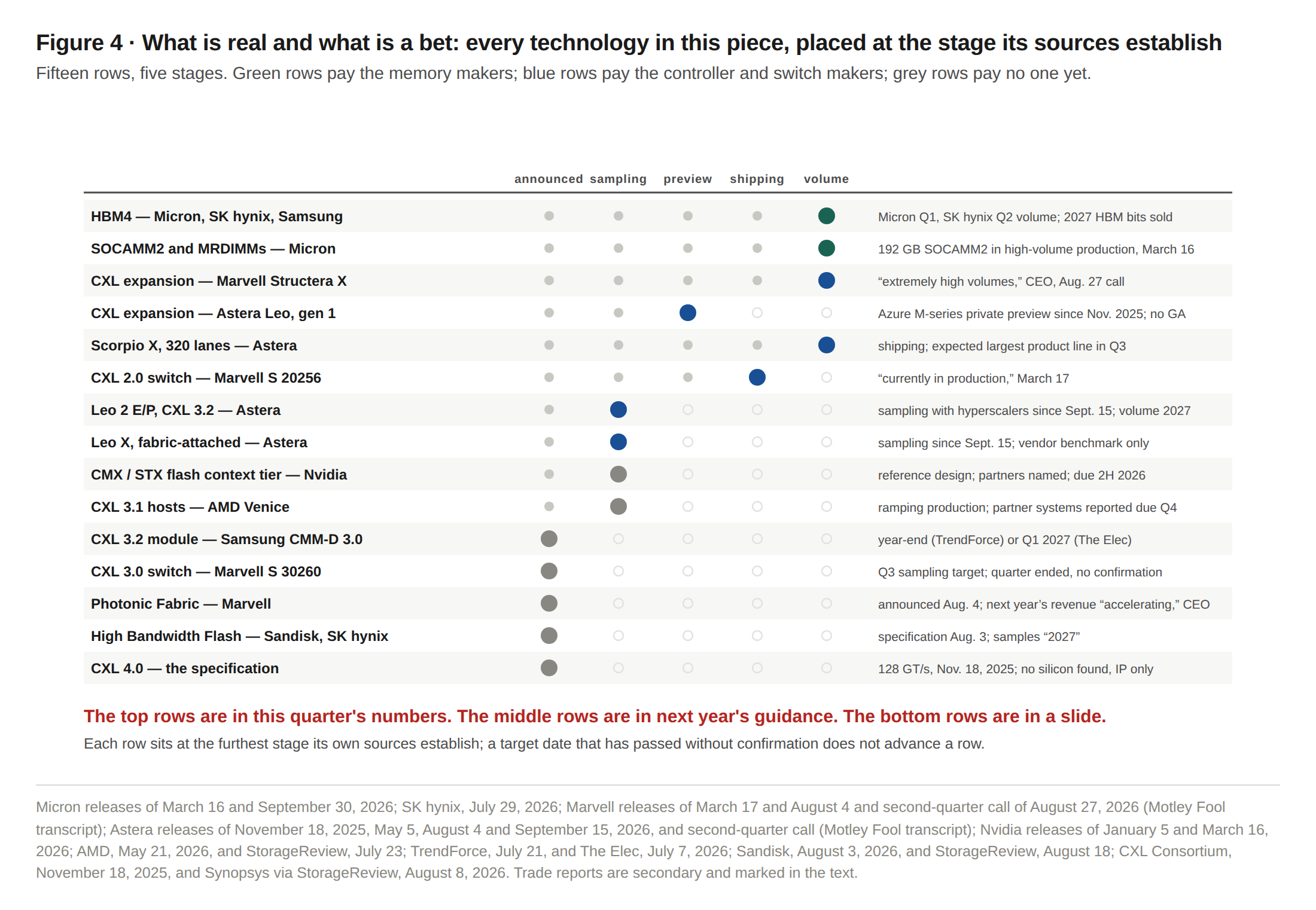
That separation is the difference between a technology thesis and an earnings model. The top row is in this quarter's numbers. The middle row is in next year's guidance. The bottom row is in a slide.
Who gets paid for the staircase?
Yesterday's piece said the owner of a bottleneck keeps the margin, its customer keeps the growth, and its middleman keeps the risk. The staircase does not change the owner.
The owner is still the memory maker, and the staircase makes the ownership more valuable, not less. Every wafer that becomes HBM is a wafer that does not become DDR5, and TrendForce puts HBM at 18, 22 and 30 percent of DRAM wafer input in 2025, 2026 and 2027 — Samsung's own executive said "nearly 30%" next year — while expecting the blended HBM price to "jump 121%" in 2027 (TrendForce, June 2 and September 29). That squeeze is why old DDR4 costs more than new DDR5, why a used-DIMM controller has a business, and why nothing on the lower steps reduces what Micron is paid. The lower steps are where buyers go when the top step is sold out, and Micron says the vast majority of next year's is already under agreement.
The controller and switch makers are paid per system, and the tape says switching is being paid for now. Astera reported $392.4 million in revenue in the June quarter, up 104 percent year over year, and guided the September quarter to $540 to $560 million — 40 percent higher at the midpoint, the desk's arithmetic — with Scorpio expected to become its largest product line in that quarter. Leo is contributing "some revenue" in the back half that "will ramp more materially into 2027" (Q2 release and call, August 4). It does not disclose revenue by product. The stock closed Wednesday at $355.97, a market value of $61.8 billion (MarketBeat and stockanalysis.com, both at the September 30 close, agreeing); it has risen 41 percent since the Leo launch on September 15, the desk's arithmetic on stockanalysis.com closes, in a period in which the company issued no further release. The market has priced in the staircase before it has shipped.
Marvell is the broader bet and the harder one to isolate. Its July quarter brought $2.739 billion of revenue, $2.17 billion of it from the data center — 79 percent, the desk's arithmetic — and a guide of $3.15 billion for the quarter ending this month (release, August 27). Its CXL business has no separate line; its chief executive promised "a very comprehensive memory expansion section" at the investor day next Tuesday, October 6 (August 27 call). The most consequential document is the one with no memory in its title: the warrant agreement Google signed on August 18, for 58,970,907 shares at $206.58, vesting mostly as Marvell's custom-silicon revenue to Google grows, with a scope that names "memory interface controllers, and near-memory compute" (Marvell 8-K, August 19). The stock closed Wednesday at $264.21, a market value of $231.7 billion (stockanalysis.com, one feed, as of the 4 p.m. close). A reader who wants to know whether the staircase pays Marvell will learn more on Tuesday than from anything in this piece.
Storage makers and software are paid last and longest. Micron's SSD line, Nvidia's partner list for CMX, Sandisk's flash stack: these are the warehouses. A warehouse earns rent for as long as the inventory exists, and the inventory in this case is every long conversation anyone is still having.
The test for all of them is the one the desk's draft proposed, and it is worth keeping in one sentence. Does the extra useful work pay for the memory, the controller, the switch, the power, the software, the qualification, and the people who run it? A database answers that one way, a recommendation engine another, an inference cluster a third. A design win does not answer it. A production order does not settle the margin. And a necessary technology does not make its supplier's stock cheap.
The dates that test this piece
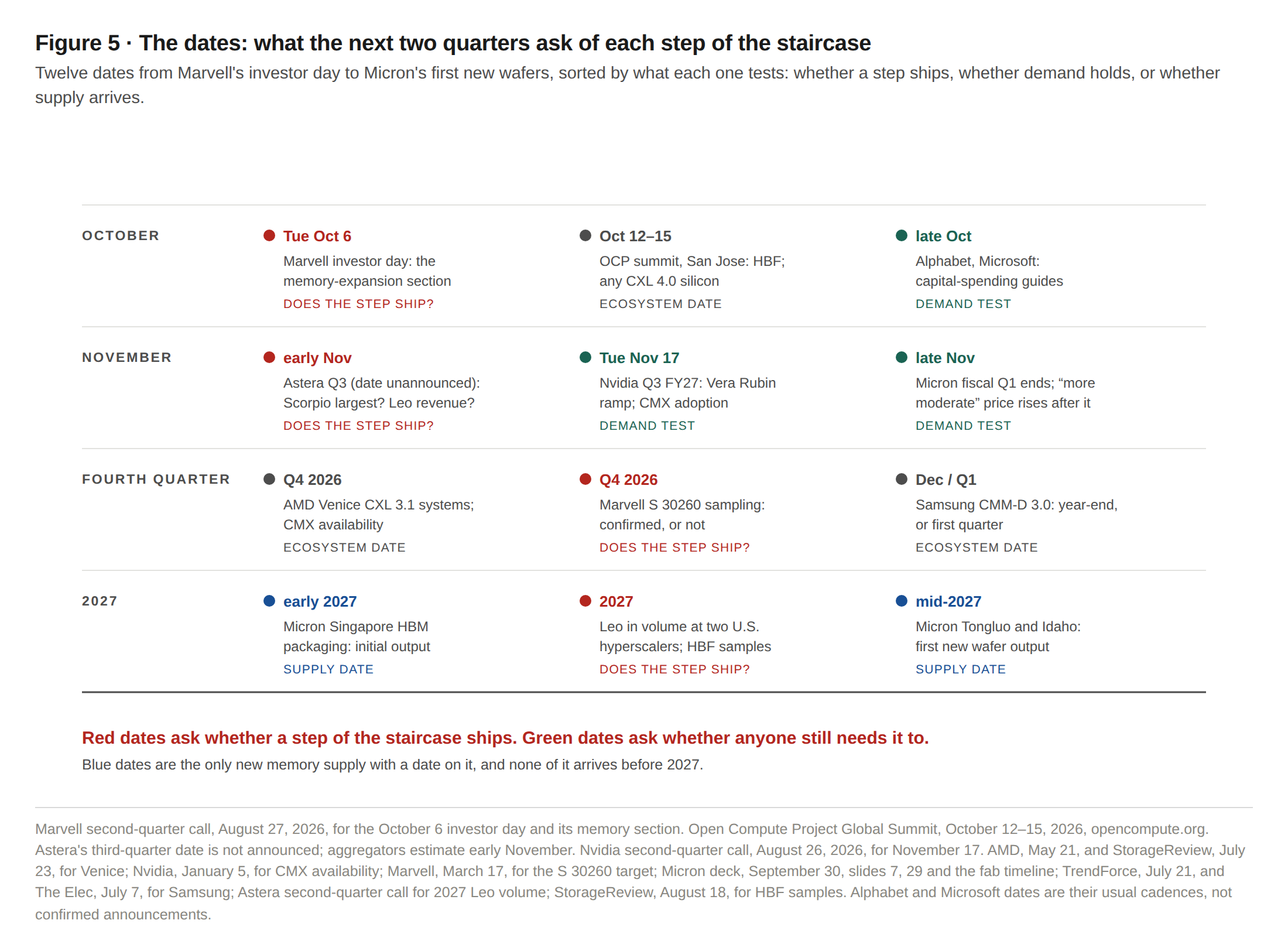
October 6, Tuesday: Marvell's investor day, with the memory-expansion section its chief executive promised. The desk will look for a CXL revenue figure or a named customer. October 12 to 15: the Open Compute Project summit in San Jose — the body through which HBF's specification was written, and the room in which any CXL 4.0 silicon would be shown. Early November, date not yet announced: Astera's third quarter — whether Scorpio became the largest line, whether Leo's "some revenue" has a number. November 17: Nvidia, with the first Vera Rubin ramp and any CMX adoption figure. This quarter: AMD's CXL 3.1 systems; CMX availability; confirmation, or not, that Marvell's new switch is sampled. Year-end: Samsung's next CXL module, or Q1. 2027: Leo in volume at two hyperscalers; HBF samples; Micron's Singapore HBM packaging line in early 2027 and its first new fab output in mid-year.
What would move the desk?
Four things, in the order they would matter.
A hyperscaler's capital-spending guide in late October coming in below its prior one. That is the demand side of every number in this piece, and nothing on the staircase survives it.
Evidence that bytes per token are falling faster than tokens per day are rising: a frontier model shipping with DeepSeek-class cache compression and a serving provider reporting lower memory per user as a result. The warehouses would still exist. They would stop growing.
A public-preview or general-availability notice for CXL memory in a major cloud — Azure's M-series preview is ten months old — or its absence through another quarter. One would move pooling from the bottom row of Figure 4 to the middle; the other would say the kernel's "known gap" is still the binding one.
And Micron's own line, from Wednesday: "a more moderate rate of price increases" beyond its fiscal first quarter, which ends in early December (deck, slide 30). If the transfer price stops rising, the lower steps lose their urgency, and the controller stocks lose their multiple before the memory maker loses a dollar.
Libraries learned this a long time ago. Not every book belongs on the desk. The craft is in knowing which ones, how far away the shelf can be, and who is paid to walk there. The AI buildout has just discovered that it is a library, and that the walk is the business.
The TrendyVest Championship is open for registration at Tournament.Trendyvest.com — 500 seats, a $100,000 simulated stake, free to enter. Trading begins today at the market open.
Sources and data notes
What the desk changed. The supplied draft was a vendor-organized technology survey; this piece is organized by tier, and the vendor material is placed where its product sits on the staircase. Three corrections run at full size where they occur: the Leo X millisecond figures, which the desk could not retrieve from Astera's blog and does not print; the HBF sample timeline, which slipped from the 2025 memorandum's dates to "2027" at Sandisk's August investor day; and the description of NVHBM, which Nvidia announced as its own custom base-die technology on August 26 — "up to 30% more memory bandwidth per stack compared with standard HBM4e" — and which Micron on September 30 said it is "working with NVIDIA on," rather than a Micron announcement (Nvidia developer blog, August 26; Micron prepared remarks, September 30). Two figures in the draft were attributed to one vendor and are from two: Rubin's bandwidth (19.2 and 22 terabytes a second, both Nvidia's) and Vera's memory capacity (1.5 terabytes per Nvidia, 2 per Micron); both are printed as found. The draft's statement that CXL 4.0's bundled ports serve memory devices is corrected: the consortium describes them as combining ports "between Host and CXL accelerators (Type 1/2 devices)." The draft's Mooncake, vLLM, LMCache, Dynamo, Gholami, DeepSeek, spot-price, warrant and investor-day material is the desk's addition. One passage of the draft, on a vendor's host-side memory-tiering mode and its roadmap, is reduced here to the documented platform facts in the CXL section.
Micron. Fiscal fourth-quarter 2026 earnings deck and prepared remarks, September 30, 2026, quoted by slide: HBM agreements and NVHBM (slide 13); SSD revenue and "AI context memory storage" (slide 13); "much tighter" (slide 4, fiscal; slide 16, calendar); "line of sight" (slide 17); gross margin (slide 27); "more moderate rate of price increases" (slide 30); fab timeline (slides 8 and 9). Fiscal 2026 ended September 3, 2026; fiscal first quarter 2027 ends December 3. Releases of March 16, 2026 (HBM4 volume shipment; SOCAMM2) and product pages for HBM4 and MRDIMM as of October 1.
Nvidia. Vera Rubin NVL72 and Vera CPU specification pages as of October 1 (the NVL72 page carries a September 30 update); developer blogs of January 5 (Rubin platform), March 16 (CMX/STX), July 21 (Rubin GPU), August 26 (NVHBM) and September 18, 2025 (Dynamo); releases of January 5 and March 16, 2026 and September 9, 2025 (Rubin CPX); Nvidia blog of August 27, 2026 (Vera shipping). Dynamo tier names from the KV Block Manager design document, v1.3.0.
Astera Labs. Releases of September 15, 2026 (Leo 2 and Leo X, with footnote), May 5, 2026 (Scorpio X 320-lane), November 18, 2025 (Azure); second-quarter 2026 release and SEC Exhibit 99.1, August 4, 2026; call via Motley Fool transcript (secondary). EE Times, September 29 (Omura; H200); ServeTheHome, September 15 (capacities); The Data Center Engineer, September 17 (all secondary). The Leo X technical blog could not be retrieved; see the correction in column.
Marvell. Releases and blog of March 17, 2026 (Structera S 30260), August 4, 2026 (memory line and Photonic Fabric), December 2, 2025 and February 2, 2026 (Celestial AI), August 27, 2026 (second-quarter fiscal 2027 results); 8-K of August 19, 2026 (Google warrant agreement); Structera product pages as of October 1; first- and second-quarter calls via Motley Fool transcripts (secondary). The Vera interoperability statement exists only as a Marvell post on X of about September 24 and is not relied on in the text.
Standards and software. CXL Consortium releases of November 18, 2025 (CXL 4.0) and webinar notes of January 15, 2026; Linux kernel documentation, driver-api/cxl, device types and maturity map, kernel 7.3 documentation; Zhong et al., "Managing Memory Tiers with CXL in Virtualized Environments," USENIX OSDI 2024; Intel technical paper 886601, February 25, 2026, and white paper 842211 (arXiv 2412.12491), December 2024; Qin et al., "Mooncake," USENIX FAST 2025; "Insights into DeepSeek-V3," ISCA 2025, arXiv 2505.09343, Table 1; Gholami et al., "AI and Memory Wall," arXiv 2403.14123; vLLM blog, January 8, 2026; LMCache technical report, arXiv 2510.09665; Hugging Face Transformers cache documentation, v5.17 (quantization) and v4.55 (sliding window); Llama 3.1 70B configuration via the NousResearch mirror of Meta's repository; Nvidia developer blog, November 17, 2023 (cache formula). AMD Turin and Venice white papers; Intel Xeon 6 product brief, May 13, 2026; StorageReview, July 23, and ServeTheHome, September 25 (Venice timing, secondary); TweakTown, May 5, 2026 (MRDIMM generation two, secondary).
Memory market. TrendForce: September 30, 2026 (fourth-quarter contract forecast; spot sheet), September 29 (2027 HBM pricing; Samsung wafer share), June 2 (HBM share of wafers and bits), July 21 (Samsung CMM-D 3.0); The Elec, July 7 (secondary). Sandisk release, August 3, 2026; SK hynix newsroom, August 4, 2026; Sandisk-SK hynix memorandum, August 6, 2025; StorageReview, August 18, 2026 (secondary). Blocks & Files, March 30, 2026 (DDN, WEKA claims; secondary).
The tape. Astera: $355.97 close, September 30, and $61.76 billion market value, MarketBeat and stockanalysis.com, agreeing; $252.54 close on September 15, stockanalysis.com. Marvell: $264.21 close, September 30, $231.69 billion, stockanalysis.com, one feed, stamped 4:00 p.m. EDT.
Arithmetic. The cache figures (327,680 bytes per token; 42.9 gigabytes at 131,072 tokens; 4.3 terabytes for one hundred sessions; fifteen Rubin GPUs; 745 conversations in 32 terabytes), the link rates (63 and 118–121 gigabytes a second per direction), the per-socket bandwidths (563 and 410 gigabytes a second), the transfer times in Figure 3, the spot prices per gigabyte ($28.95 and $41.84; 45 percent), the 48 percent uncontended figure, Astera's 40 percent guide step and 41 percent move, and Marvell's 79 percent data-center share are the desk's calculations from the printed inputs. Gigabytes are decimal throughout; the 42.9-gigabyte figure is 40 gibibytes. We checked the weekdays named in the text against the calendar.
Disclosure. This desk's tooling is built on Claude, made by Anthropic; Anthropic is not named in this piece.